
New

FPGA Development Workbench


₹ 0.00
In StockFPGA Development Workbench is an integrated engineering platform designed for FPGA design, digital logic development, RTL concepts, hardware simulation, verification, and programmable logic learning. It provides an interactive environment for exploring digital circuits, combinational and sequential logic, Verilog/VHDL design concepts, FPGA architectures, and hardware development workflows. Ideal for electronics engineers, FPGA developers, embedded system designers, researchers, trainers, and students. A free demo is available for a few days, allowing users to explore the workbench and experience its capabilities before purchasing.
Description
FPGA Development Workbench – Complete FPGA Design, Simulation & Digital Hardware Engineering Platform
FPGA Development Workbench is a comprehensive engineering and learning platform designed to support Field Programmable Gate Array (FPGA) development, digital logic design, hardware architecture exploration, simulation, and verification. It provides an integrated environment for understanding programmable hardware technologies, developing digital circuit concepts, exploring RTL design methodologies, and learning the fundamental principles of FPGA-based system development.
Designed for electronics engineers, FPGA developers, embedded systems professionals, hardware designers, researchers, engineering institutions, trainers, and students, FPGA Development Workbench bridges the gap between theoretical digital electronics and practical hardware engineering. It offers an interactive environment to explore digital logic concepts, understand hardware design workflows, analyze circuit behavior, and develop knowledge of FPGA implementation methodologies.
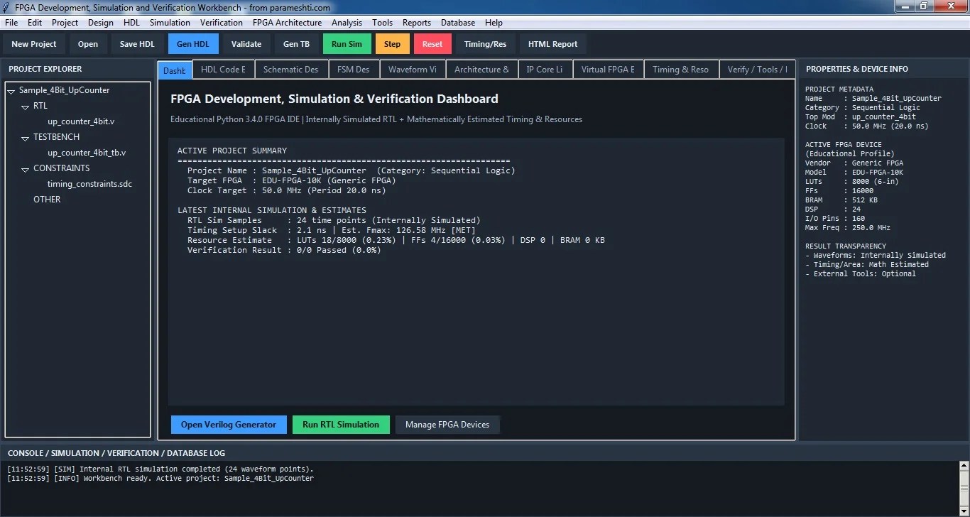
Comprehensive FPGA Development Environment
The workbench covers important areas of FPGA and digital hardware engineering, providing users with opportunities to explore the design process from fundamental digital logic concepts to advanced programmable hardware architectures.
Key engineering and learning areas include:
- Digital Logic Design: Explore fundamental digital electronics concepts, including logic gates, Boolean algebra, truth tables, logic expressions, and digital circuit implementation.
- Combinational Circuit Design: Understand multiplexers, demultiplexers, encoders, decoders, comparators, adders, subtractors, and other combinational logic circuits.
- Sequential Logic Design: Study flip-flops, registers, counters, shift registers, finite state machines, and clock-driven digital circuit behavior.
- Verilog HDL Development: Explore Hardware Description Language concepts, RTL coding structures, modules, ports, operators, procedural blocks, and digital hardware modeling using Verilog.
- VHDL Development: Understand VHDL design methodologies, entity and architecture structures, signal declarations, processes, concurrent statements, and hardware description techniques.
- FPGA Architecture Exploration: Learn FPGA architecture concepts, including configurable logic blocks, lookup tables (LUTs), flip-flops, programmable interconnects, input/output blocks, and embedded resources.
- RTL Design and Simulation: Understand Register Transfer Level (RTL) design methodologies and explore how hardware functionality can be represented and evaluated through simulation.
- Testbench and Functional Verification: Explore testbench development, stimulus generation, functional verification, waveform analysis, and the importance of validating digital hardware designs.
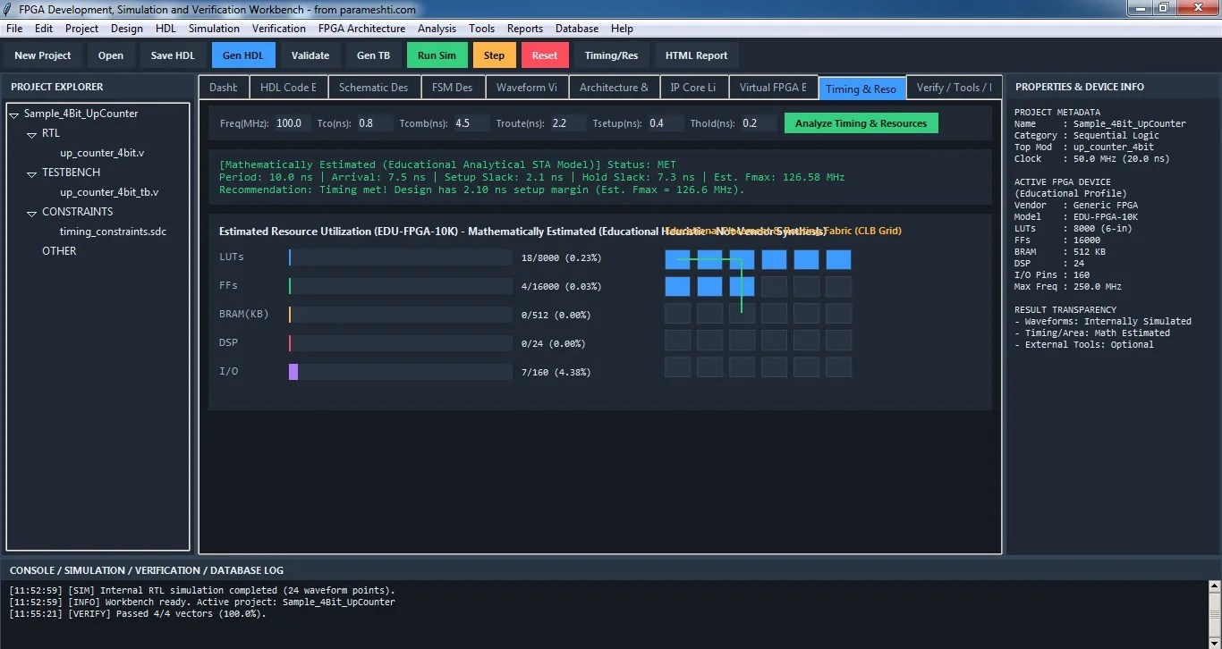
- Timing and Clock Analysis: Understand clock signals, propagation delay, setup time, hold time, timing constraints, and timing-related considerations in synchronous digital systems.
- FPGA Design and Implementation Workflow: Explore the FPGA development lifecycle, including design entry, synthesis, technology mapping, placement, routing, implementation, and programming concepts.
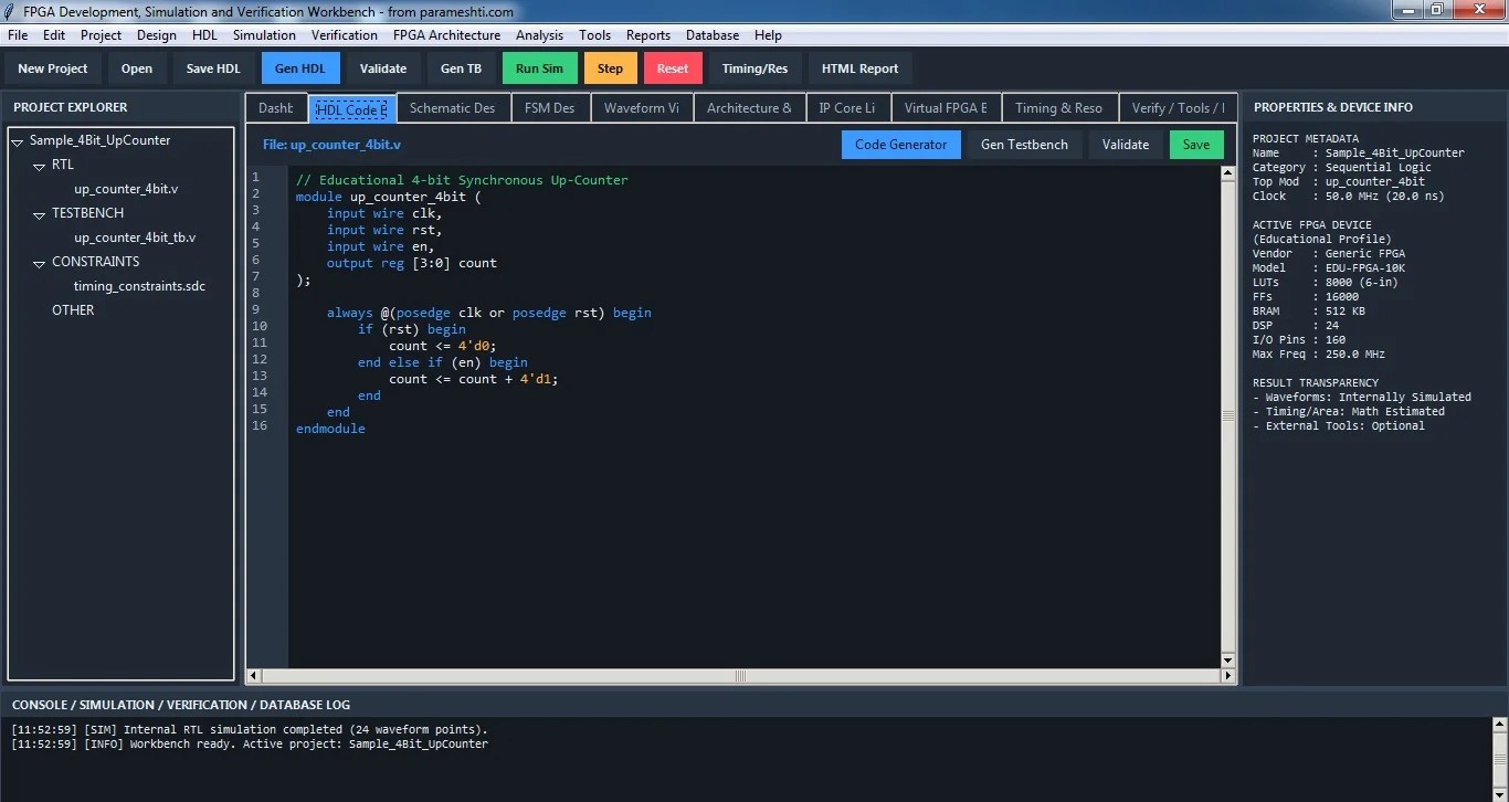
Practical Learning and Engineering Applications
FPGA Development Workbench provides an integrated environment for understanding digital hardware development and programmable logic engineering. Users can explore circuit design concepts, investigate digital system behavior, understand HDL-based design methodologies, and develop practical knowledge of FPGA engineering workflows.
It is suitable for learning applications involving digital signal processing, embedded systems, communication systems, control systems, industrial automation, and hardware acceleration.
The workbench can support academic laboratory activities, engineering training, technical demonstrations, self-learning, and research-oriented exploration of FPGA technologies.
Who Can Benefit?
- FPGA and digital hardware design engineers.
- Electronics and electrical engineering professionals.
- Embedded systems developers.
- Verilog and VHDL learners.
- Digital design and hardware verification engineers.
- Engineering colleges and universities.
- Technical training institutes and research organizations.
- Students pursuing electronics, communication, and computer engineering.
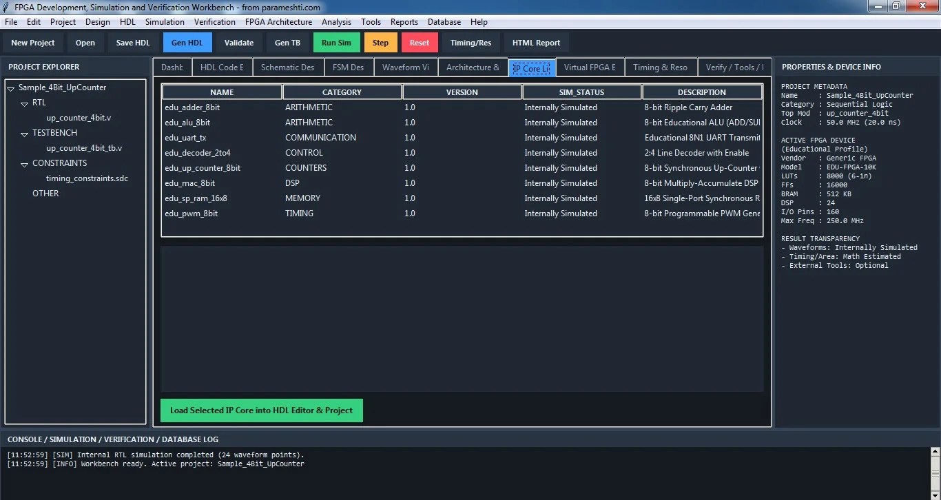
Try Before You Buy – Free Demo Available
Explore FPGA Development Workbench before making a purchase!
A free demo is available for a few days, giving prospective users an opportunity to experience the platform, explore its features, understand its engineering capabilities, and evaluate its suitability for their learning, development, or training requirements.
The demo provides an excellent opportunity for individuals, engineering teams, academic institutions, and organizations to discover the value of the workbench before opting for the full version.
Your Complete Workbench for FPGA Engineering
Whether you are learning digital logic design, developing Verilog or VHDL knowledge, exploring FPGA architectures, studying RTL methodologies, or building expertise in programmable hardware systems, FPGA Development Workbench provides a versatile engineering environment to support your objectives.
FPGA Development Workbench – Design Smarter. Simulate Better. Build the Future of Programmable Hardware.
Related products
-
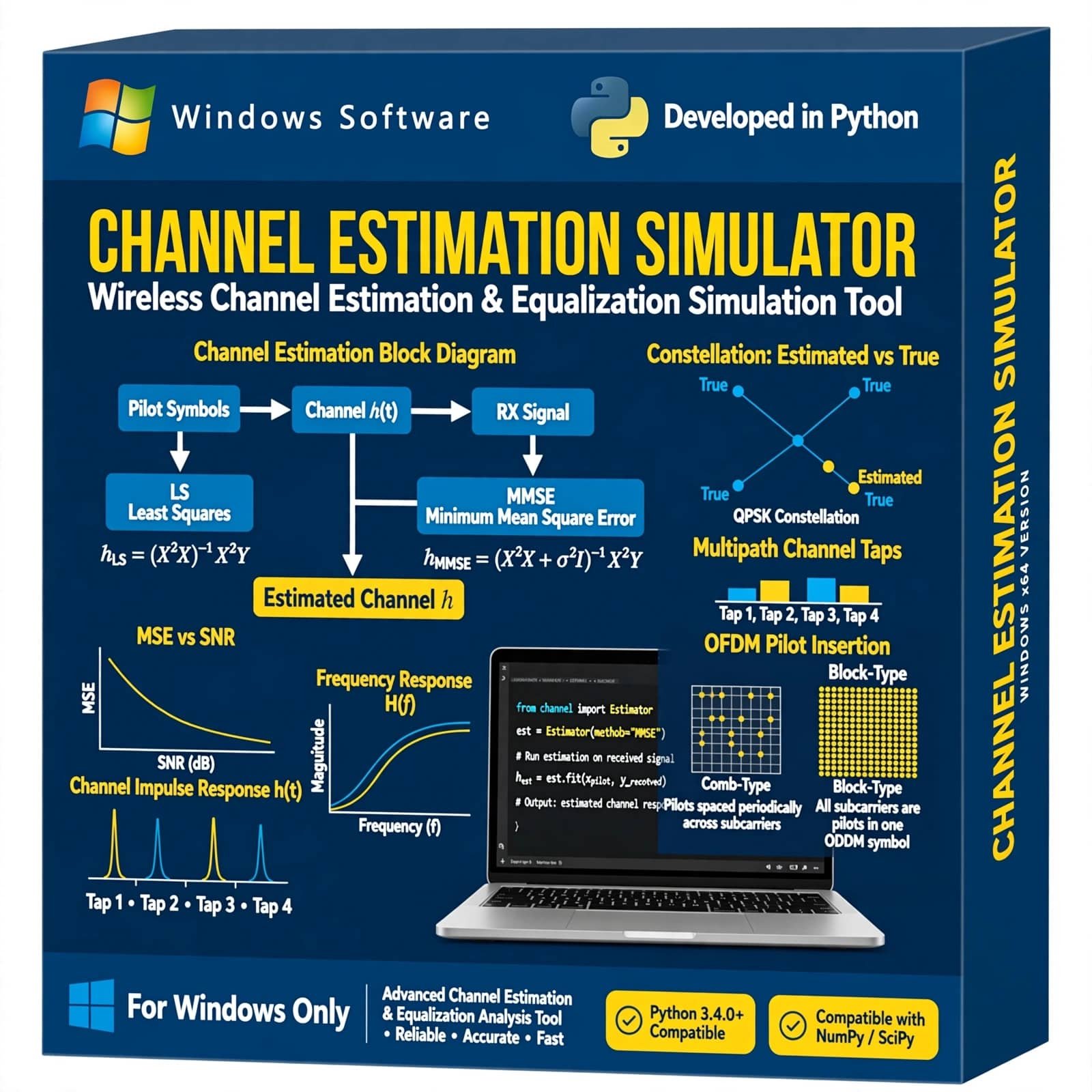
Channel Estimation Simulator is a wireless communication simulation tool designed to demonstrate and analyze channel estimation techniques in digital communication systems. It helps students, researchers, and communication engineers study channel effects, pilot-based estimation, signal distortion, and estimation performance through practical simulation.
₹ 249.00 -
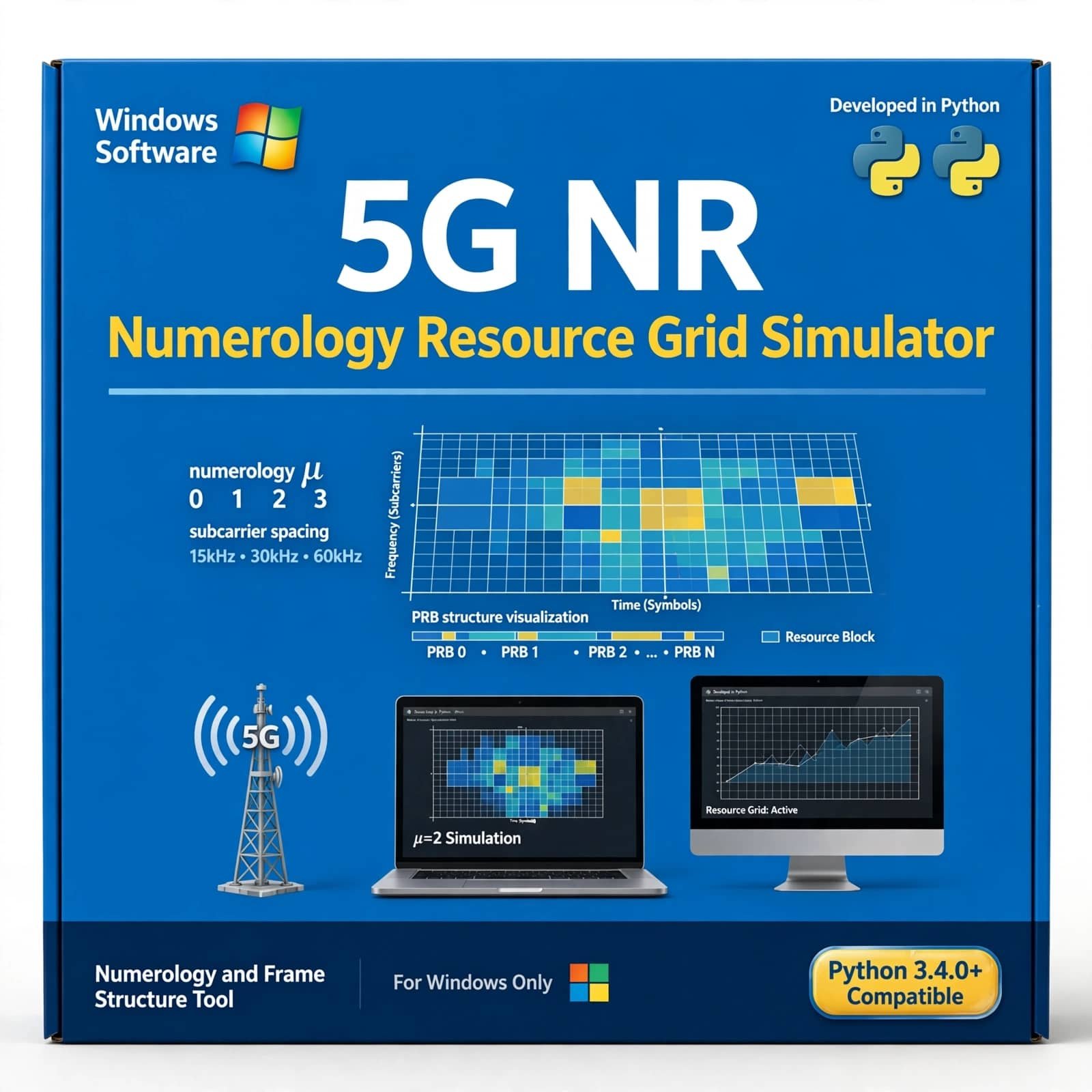
5G NR Numerology Resource Grid Simulator is an advanced simulation solution for modeling and analyzing 5G New Radio numerology and time-frequency resource grid structures. It enables users to study subcarrier spacing, OFDM symbols, slot structure, cyclic prefix, Physical Resource Blocks (PRBs), Resource Elements (REs), bandwidth configurations, and resource mapping. The simulator is ideal for 5G NR physical-layer research, numerology analysis, resource allocation studies, academic projects, waveform development, and 5G/6G wireless communication research.
₹ 2,299.00 -
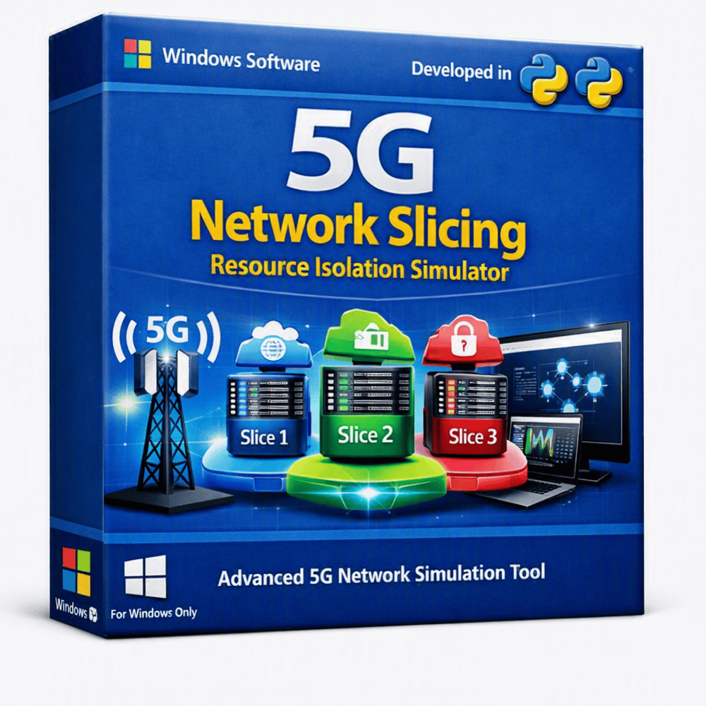
A Python-based 5G Network Slicing and Resource Isolation Simulator designed to model and analyze how multiple logical network slices can share physical 5G infrastructure while maintaining resource isolation. The simulator enables users to study CPU, memory, bandwidth, network capacity, traffic allocation, and resource management across different 5G network slices.
Ideal for 5G research, telecom engineering, academic projects, network optimization, resource allocation studies, and university laboratories.
₹ 1,999.00 -
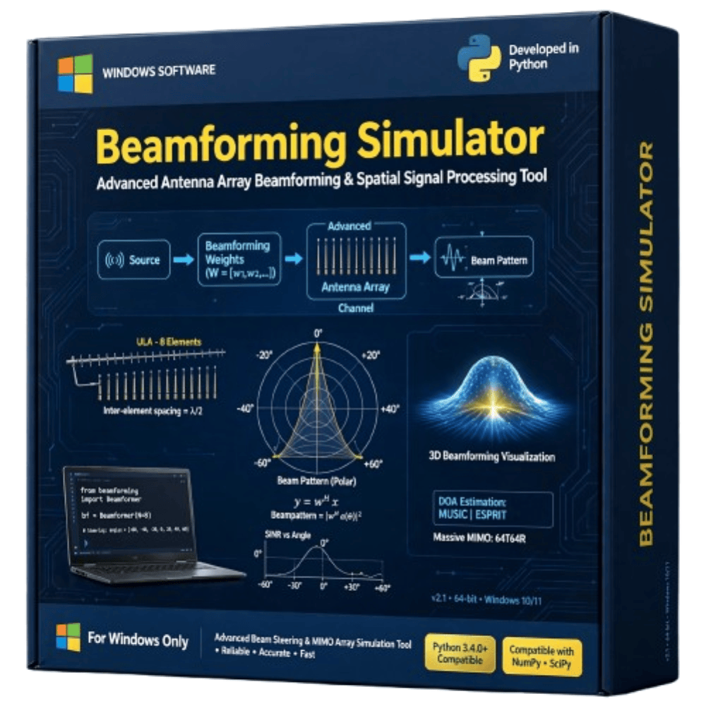
The Beamforming Simulator is a practical wireless communication simulation project designed to demonstrate how antenna arrays can control and direct radio-frequency signals toward desired users or directions. The simulator helps visualize beam patterns, signal direction, antenna-array behavior, and beam steering under different parameters. It is suitable for studying beamforming, antenna arrays, MIMO, 5G communication, wireless networks, and signal processing. This project is ideal for engineering students, researchers, and learners working on wireless communication and advanced antenna technologies.
₹ 1,299.00 -
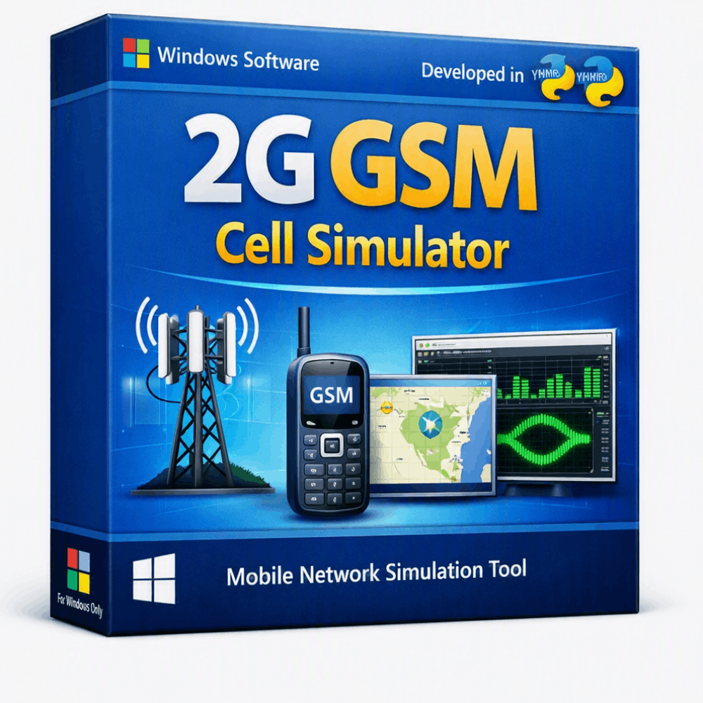
The 2G GSM Cell Simulator is a Python-based software project designed to simulate fundamental GSM cellular-network concepts. It provides a practical environment for understanding mobile stations, GSM cells, base stations, cellular coverage, mobility, communication channels, and basic network behavior. The project includes Python source code that can be studied, customized, and extended for academic projects, demonstrations, research, and learning. It is ideal for Electronics & Communication Engineering, Telecommunications, Computer Science, and related students looking to explore 2G GSM technology and cellular network simulation through a software-based implementation.
₹ 999.00 -
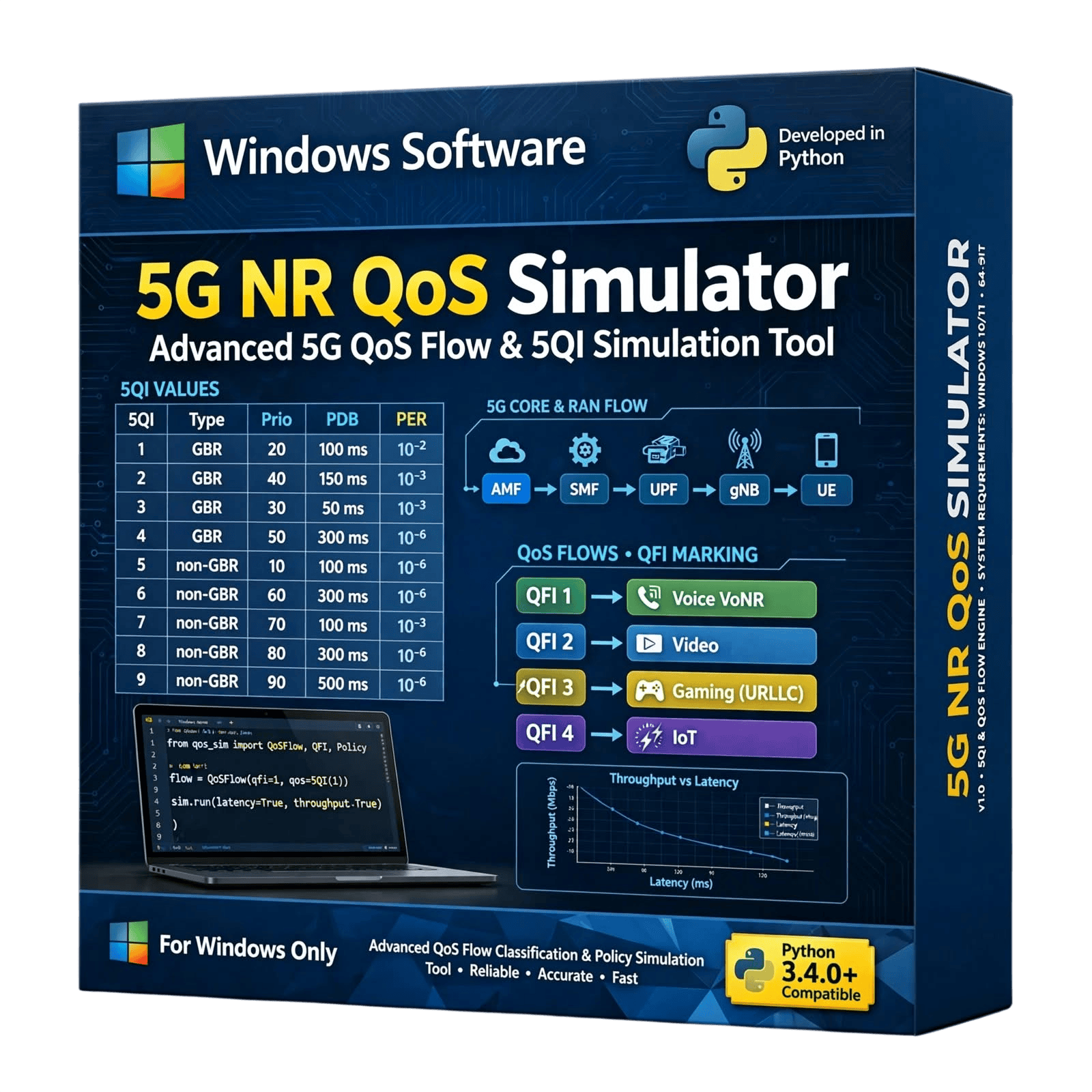
The 5G QoS Simulator is a Python-based software solution designed for researchers, engineers, students, developers, and telecommunications professionals working with 5G Quality of Service (QoS) concepts. The simulator provides a software-based environment for studying and analyzing QoS-related aspects of 5G communication networks, including service performance, traffic behavior, resource management, and network performance evaluation.
Developed using Python, the simulator is suitable for academic research, telecommunications projects, demonstrations, experimentation, algorithm development, and educational applications.
Available for sale as a software product. Contact us for pricing, licensing, features, customization, and purchase information.
₹ 2,299.00


Reviews
There are no reviews yet.